

-
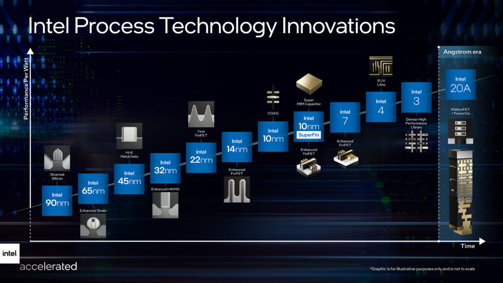
Intel’s graph of the past and future. [credit: Intel ]
Earlier this year, Intel got a new CEO and kicked off a new business plan that would open its foundries to other chip-design firms, just like how TSMC and Samsung Semiconductor operate. At its “Intel Accelerated” event today, the company laid out a roadmap for its future as a for-hire foundry. Besides the future of ever-smaller process nodes, the company also announced it has scored one of the world’s biggest chip designers, Qualcomm, as a future foundry customer.
As part of entering the foundry market, Intel will start naming its process nodes more like its rivals. The process-node numbers used for chips like “5nm” started out life as a measurement of transistor size, but eventually the marketers got hold of them and companies started cheating down their numbers to look more advanced. Intel says its new naming scheme will better align with how TSMC and Samsung talk about their foundry technologies. Gone are the days of “Intel 10nm Enhanced Super Fin”—instead, the node is called “Intel 7.” It should have a comparable density to the TSMC and Samsung 7 nm nodes and will be ready for production in Q1 2022 (TSMC and Samsung are currently shipping “5nm” products). “Intel 4″—which Intel previously called “7nm”—is now said to be equivalent to TSMC and Samsung’s 4 nm node, and it will begin manufacturing products in 2023.
If you’re wondering what happens when we run out of “nm” numbers, Intel’s sales pitch for that is the “Angstrom” era, a unit of measurement that is one-tenth of a nanometer. In 2024, the company wants to ramp up the “Intel 20A” process node (so a “2nm” equivalent, but Intel was calling this node “5nm” previously, but remember these are marketing numbers and not really units of measurement). In early, 2025 the company will be working on “Intel 18A.”
Read 3 remaining paragraphs | Comments